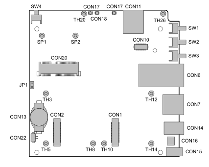
第11章 Interface SpecificationsThe following explains the interface specifications of Armadillo-IoT. 表11.1 Armadillo-IoT Interface List (Side A)[] | Part Number | Interface Name | Product Number | Maker |
|---|
| CON1 | Add-on Interface 1 | DF17(4.0)-60DS-0.5V(57) | HIROSE ELECTRIC | | CON2 | Add-on Interface 2 | DF17(4.0)-60DS-0.5V(57) | HIROSE ELECTRIC | | CON6 | LAN Interface | 9771-8813-S3L6T1 | SUN JUN ELECTRONICS | | CON7 | USB Host Interface | UBA-4R-D14T-4D(LF)(SN) | J.S.T. Mfg. | | CON10 | WWAN Expansion Interface | DF12(3.0)-30DP-0.5V(86) | HIROSE ELECTRIC | | CON11 | MicroSIM Interface | CIM-J78 | MITSUMI | | CON13 | RTC Backup Interface 1 | SMTU1220-LF | Renata SA | | CON14 | Power Input Interface 1 | PJ-102AH | CUI | | CON15 | Power Input Interface 2 | S02B-PASK-2(LF)(SN) | J.S.T. Mfg. | | CON16 | Power Output Interface | B02B-PASK(LF)(SN) | J.S.T. Mfg. | | CON17 | 3G/LTE Antenna Interface1 | U.FL-R-SMT-1 | HIROSE ELECTRIC | | CON18 | 3G/LTE Antenna Interface2 | U.FL-R-SMT-1 | HIROSE ELECTRIC | | CON20 | WLAN Interface | MM60-52B1-E1-R650 | Japan Aviation Electronics Industry | | CON22 | RTC Backup Interface 2 | DF13C-2P-1.25V (21) | HIROSE ELECTRIC | | SW1 | User Switch 1 | SKHHLRA010 | ALPS ELECTRIC | | SW2 | User Switch 2 | SKHHLRA010 | ALPS ELECTRIC | | SW3 | User Switch 3 | SKHHLRA010 | ALPS ELECTRIC | | SW4 | Reset Switch | SKHHLUA010 | ALPS ELECTRIC | | JP1 | Boot Device Configuration Jumper | A2-2PA-2.54DSA(71) | HIROSE ELECTRIC | | TH3 | Stud for Add-on Module | KRB-2008 | Hirosugi-Keiki | | TH5 | | TH8 | | TH10 | | TH12 | | TH14 | | TH20 | Stud for WWAN Module | TH-1.6-3.0-M2 | Mac-Eight | | TH26 | | SP1 | Stud for Wireless LAN Module | NT4R1600 | Japan Aviation Electronics Industry | | SP2 |
![[警告]](images/warning.png) | |
|---|
The is no guarantee that the parts installed have the part numbers shown in 表11.1「Armadillo-IoT Interface List (Side A)」. Please check the parts specifications and change history table which can be downloaded from the Atmark Techno Users' site for the parts on your product. |
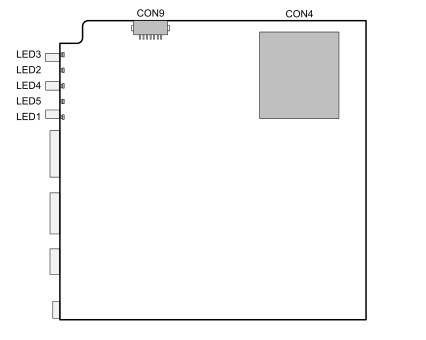
表11.2 Armadillo-IoT Interface List (Side B) | Part Number | Interface Name | Product Number | Maker |
|---|
| CON4 | SD Interface | DM1B-DSF-PEJ(82) | HIROSE ELECTRIC | | CON9 | Debug Serial Interface | DF13A-7P-1.25H(51) | HIROSE ELECTRIC | | LED1 | WWAN LED | SML-A12P8T | ROHM | | LED2 | User LED2 | SML-A12P8T | ROHM | | LED3 | User LED1 | SML-A12P8T | ROHM | | LED4 | User LED3 | SML-A12P8T | ROHM | | LED5 | User LED4 | SML-A12P8T | ROHM |
| |
|---|
The is no guarantee that the parts installed have the part numbers shown in 表11.2「Armadillo-IoT Interface List (Side B)」. Please check the parts specifications and change history table which can be downloaded from the Atmark Techno Users' site for the parts on your product. |
11.2. CON1 Add-on Interface 1CON1 is an expansion interface. It connects to signal lines of the i.MX7 Dual which offer multiple functions (multiplexing), and functions such as USB, UART, SPI, I2C, SD, CAN, PWM and GPIO can be interfaced to. - Mounted Connector
DF17(4.0)-60DS-0.5V(57)/HIROSE ELECTRIC - Matching Connector Example
DF17(4.0)-60DP-0.5V(57)/HIROSE ELECTRIC - Allowable Current
0.3A (per one terminal)
表11.3 CON1 Signals | Pin Number | Pin Name | I/O | Description |
|---|
| 1 | GND | Power | Power (GND) | | 2 | GND | Power | Power (GND) | | 3 | GPIO3_IO0 | In/Out |
Expansion I/O, connected to LCD_CLK pin of i.MX7 Dual
Shared connection with pin 41 of CON2
| | 4 | GPIO3_IO1 | In/Out |
Expansion I/O, connected to LCD_ENABLE pin of i.MX7 Dual
Shared connection with pin 40 of CON2
| | 5 | GPIO3_IO2 | In/Out |
Expansion I/O, connected to LCD_HSYNC pin of i.MX7 Dual
Shared connection with pin 39 of CON2
| | 6 | GPIO3_IO3 | In/Out |
Expansion I/O, connected to LCD_VSYNC pin of i.MX7 Dual
Shared connection with pin 38 of CON2
| | 7 | GPIO4_IO2 | In/Out |
Expansion I/O, connected to UART2_RXD pin of i.MX7 Dual
Shared connection with pin 32 of CON2
| | 8 | GPIO4_IO3 | In/Out |
Expansion I/O, connected to UART2_TXD pin of i.MX7 Dual
Shared connection with pin 34 of CON2
| | 9 | GPIO4_IO4 | In/Out |
Expansion I/O, connected to UART3_RXD pin of i.MX7 Dual
Shared connection with pin 36 of CON2
| | 10 | GPIO4_IO5 | In/Out |
Expansion I/O, connected to UART3_TXD pin of i.MX7 Dual
Shared connection with pin 37 of CON2
| | 11 | GPIO4_IO6 | In/Out |
Expansion I/O, connected to UART3_RTS pin of i.MX7 Dual
Shared connection with pin 35 of CON2
| | 12 | GPIO4_IO7 | In/Out |
Expansion I/O, connected to UART3_CTS pin of i.MX7 Dual
Shared connection with pin 50 of CON2
| | 13 | GPIO4_IO10 | In/Out |
Expansion I/O, connected to I2C2_SCL pin of i.MX7 Dual
Shared connection with pin 24 of CON2
| | 14 | GPIO4_IO11 | In/Out |
Expansion I/O, connected to I2C2_SDA pin of i.MX7 Dual
Shared connection with pin 25 of CON2
| | 15 | GPIO5_IO11 | In/Out |
Expansion I/O, connected to SD2_RESET_B pin of i.MX7 Dual
Shared connection with pin 33 of CON2
| | 16 | GPIO6_IO19 | In/Out |
Expansion I/O, connected to SAI2_TXFS pin of i.MX7 Dual
Shared connection with pin 46 of CON2
| | 17 | GPIO6_IO20 | In/Out |
Expansion I/O, connected to SAI2_TXC pin of i.MX7 Dual
Shared connection with pin 47 of CON2
| | 18 | GPIO6_IO22 | In/Out |
Expansion I/O, connected to SAI2_TXD pin of i.MX7 Dual
Shared connection with pin 49 of CON2
| | 19 | GPIO6_IO21 | In/Out |
Expansion I/O, connected to SAI2_RXD pin of i.MX7 Dual
Shared connection with pin 48 of CON2
| | 20 | GPIO4_IO8 | In/Out |
Expansion I/O, connected to I2C1_SCL pin of i.MX7 Dual
Shared connection with pin 20 of CON2
| | 21 | GPIO4_IO9 | In/Out |
Expansion I/O, connected to I2C1_SDA pin of i.MX7 Dual
Shared connection with pin 21 of CON2
| | 22 | GPIO4_IO12 | In/Out |
Expansion I/O, connected to I2C3_SCL pin of i.MX7 Dual
Shared connection with pin 42 of CON2
| | 23 | GPIO4_IO13 | In/Out |
Expansion I/O, connected to I2C3_SDA pin of i.MX7 Dual
Shared connection with pin 43 of CON2
| | 24 | GPIO3_IO25 | In/Out | Expansion I/O, connected to LCD_DATA20 pin of i.MX7 Dual | | 25 | GPIO3_IO26 | In/Out | Expansion I/O, connected to LCD_DATA21 pin of i.MX7 Dual | | 26 | GND | Power | Power (GND) | | 27 | GND | Power | Power (GND) | | 28 | VCC_3.3V_IO | Power | Power (VCC_3.3V_IO) | | 29 | VCC_3.3V | Power | Power (VCC_3.3V) | | 30 | VCC_5V | Power | Power (VCC_5V) | | 31 | DETECT_CON1 | Out | Connected to GND with 1kΩ resistor | | 32 | GPIO7_IO12 | In/Out | Expansion I/O, connected to ENET1_TX_CLK pin of i.MX7 Dual | | 33 | GPIO7_IO13 | In/Out | Expansion I/O, connected to ENET1_RX_CLK pin of i.MX7 Dual | | 34 | GPIO7_IO7 | In/Out | Expansion I/O, connected to ENET1_TD1 pin of i.MX7 Dual | | 35 | GPIO7_IO2 | In/Out | Expansion I/O, connected to ENET1_RD2 pin of i.MX7 Dual | | 36 | GPIO7_IO8 | In/Out | Expansion I/O, connected to ENET1_TD2 pin of i.MX7 Dual | | 37 | GPIO7_IO3 | In/Out | Expansion I/O, connected to ENET1_RD3 pin of i.MX7 Dual | | 38 | GPIO7_IO0 | In/Out | Expansion I/O, connected to ENET1_RD0 pin of i.MX7 Dual | | 39 | GPIO7_IO1 | In/Out | Expansion I/O, connected to ENET1_RD1 pin of i.MX7 Dual | | 40 | GPIO4_IO1 | In/Out | Expansion I/O, connected to UART1_TXD pin of i.MX7 Dual | | 41 | GPIO4_IO0 | In/Out | Expansion I/O, connected to UART1_RXD pin of i.MX7 Dual | | 42 | GPIO7_IO4 | In/Out | Expansion I/O, connected to ENET1_RX_CTL pin of i.MX7 Dual | | 43 | GPIO7_IO5 | In/Out | Expansion I/O, connected to ENET1_RXC pin of i.MX7 Dual | | 44 | GPIO7_IO6 | In/Out | Expansion I/O, connected to ENET1_TD0 pin of i.MX7 Dual | | 45 | GPIO7_IO10 | In/Out | Expansion I/O, connected to ENET1_TX_CTL pin of i.MX7 Dual | | 46 | GPIO7_IO11 | In/Out | Expansion I/O, connected to ENET1_TXC pin of i.MX7 Dual | | 47 | GPIO5_IO12 | In/Out | Expansion I/O, connected to SD2_CLK pin of i.MX7 Dual | | 48 | GPIO5_IO13 | In/Out | Expansion I/O, connected to SD2_CMD pin of i.MX7 Dual | | 49 | GPIO5_IO14 | In/Out | Expansion I/O, connected to SD2_DATA0 pin of i.MX7 Dual | | 50 | GPIO7_IO9 | In/Out | Expansion I/O, connected to ENET1_TD3 pin of i.MX7 Dual | | 51 | GPIO5_IO15 | In/Out | Expansion I/O, connected to SD2_DATA1 pin of i.MX7 Dual | | 52 | GPIO5_IO16 | In/Out | Expansion I/O, connected to SD2_DATA2 pin of i.MX7 Dual | | 53 | GPIO5_IO17 | In/Out | Expansion I/O, connected to SD2_DATA3 pin of i.MX7 Dual | | 54 | GND | Power | Power (GND) | | 55 | PMIC_ONOFF | In | The power management IC on/off signal. Please input an open drain (or open collector) signal. | | 56 | CON1_USB_VBUS | Power | Power (CON1_USB_VBUS) | | 57 | CON1_USB_VBUS | Power | Power (CON1_USB_VBUS) | | 58 | GND | Power | Power (GND) | | 59 | CON1_USB_HS_DP | In/Out | CON1_USB plus side signal, connected to USB_OTG2_DP pin of i.MX7 Dual | | 60 | CON1_USB_HS_DM | In/Out | CON1_USB minus side signal, connected to USB_OTG2_DN pin of i.MX7 Dual |
![[ティップ]](images/tip.png) | |
|---|
There are a number of add-on modules available which can be connected. |
| |
|---|
There are many signals which connect to both CON1 and CON2. Please be careful of possible signal conflicts when designing an expansion board. |
11.3. CON2 Add-on Interface 2CON2 is an expansion interface. It connects to signal lines of the i.MX7 Dual which offer multiple functions (multiplexing), and functions such as USB, UART, SPI, I2C, and GPIO can be interfaced to. - Mounted Connector
DF17(4.0)-60DS-0.5V(57)/HIROSE ELECTRIC - Matching Connector Example
DF17(4.0)-60DP-0.5V(57)/HIROSE ELECTRIC - Allowable Current
0.3A (per one terminal)
表11.4 CON2 Signals | Pin Number | Pin Name | I/O | Description |
|---|
| 1 | GND | Power | Power (GND) | | 2 | GND | Power | Power (GND) | | 3 | NC | - | Not Connected | | 4 | NC | - | Not Connected | | 5 | NC | - | Not Connected | | 6 | NC | - | Not Connected | | 7 | NC | - | Not Connected | | 8 | NC | - | Not Connected | | 9 | NC | - | Not Connected | | 10 | NC | - | Not Connected | | 11 | NC | - | Not Connected | | 12 | NC | - | Not Connected | | 13 | NC | - | Not Connected | | 14 | NC | - | Not Connected | | 15 | NC | - | Not Connected | | 16 | NC | - | Not Connected | | 17 | NC | - | Not Connected | | 18 | NC | - | Not Connected | | 19 | NC | - | Not Connected | | 20 | GPIO4_IO8 | In/Out |
Expansion I/O, connected to I2C1_SCL pin of i.MX7 Dual
Shared connection with pin 20 of CON1
| | 21 | GPIO4_IO9 | In/Out |
Expansion I/O, connected to I2C1_SDA pin of i.MX7 Dual
Shared connection with pin 21 of CON1
| | 22 | NC | - | Not Connected | | 23 | NC | - | Not Connected | | 24 | GPIO4_IO10 | In/Out |
Expansion I/O, connected to I2C2_SCL pin of i.MX7 Dual
Shared connection with pin 13 of CON1
| | 25 | GPIO4_IO11 | In/Out |
Expansion I/O, connected to I2C2_SDA pin of i.MX7 Dual
Shared connection with pin 14 of CON1
| | 26 | GND | Power | Power (GND) | | 27 | GND | Power | Power (GND) | | 28 | VCC_3.3V_IO | Power | Power (VCC_3.3V_IO) | | 29 | VCC_3.3V | Power | Power (VCC_3.3V) | | 30 | VCC_5V | Power | Power (VCC_5V) | | 31 | DETECT_CON2 | Out | Connected to VCC_3.3 V_IO with 1kΩ resistor | | 32 | GPIO4_IO2 | In/Out |
Expansion I/O, connected to UART2_RXD pin of i.MX7 Dual
Shared connection with pin 7 of CON1
| | 33 | GPIO5_IO11 | In/Out |
Expansion I/O, connected to SD2_RESET_B pin of i.MX7 Dual
Shared connection with pin 15 of CON1
| | 34 | GPIO4_IO2 | In/Out |
Expansion I/O, connected to UART2_TXD pin of i.MX7 Dual
Shared connection with pin 8 of CON1
| | 35 | GPIO4_IO6 | In/Out |
Expansion I/O, connected to UART3_RTS pin of i.MX7 Dual
Shared connection with pin 11 of CON1
| | 36 | GPIO4_IO4 | In/Out |
Expansion I/O, connected to UART3_RXD pin of i.MX7 Dual
Shared connection with pin 9 of CON1
| | 37 | GPIO4_IO5 | In/Out |
Expansion I/O, connected to UART3_TXD pin of i.MX7 Dual
Shared connection with pin 10 of CON1
| | 38 | GPIO3_IO3 | In/Out |
Expansion I/O, connected to LCD_VSYNC pin of i.MX7 Dual
Shared connection with pin 6 of CON1
| | 39 | GPIO3_IO2 | In/Out |
Expansion I/O, connected to LCD_HSYNC pin of i.MX7 Dual
Shared connection with pin 5 of CON1
| | 40 | GPIO3_IO1 | In/Out |
Expansion I/O, connected to LCD_ENABLE pin of i.MX7 Dual
Shared connection with pin 4 of CON1
| | 41 | GPIO3_IO0 | In/Out |
Expansion I/O, connected to LCD_CLK pin of i.MX7 Dual
Shared connection with pin 3 of CON1
| | 42 | GPIO4_IO12 | In/Out |
Expansion I/O, connected to I2C3_SCL pin of i.MX7 Dual
Shared connection with pin 22 of CON1
| | 43 | GPIO4_IO13 | In/Out |
Expansion I/O, connected to I2C3_SDA pin of i.MX7 Dual
Shared connection with pin 23 of CON1
| | 44 | NC | - | Not Connected | | 45 | NC | - | Not Connected | | 46 | GPIO6_IO19 | In/Out |
Expansion I/O, connected to SAI2_TXFS pin of i.MX7 Dual
Shared connection with pin 16 of CON1
| | 47 | GPIO6_IO20 | In/Out |
Expansion I/O, connected to SAI2_TXC pin of i.MX7 Dual
Shared connection with pin 17 of CON1
| | 48 | GPIO6_IO21 | In/Out |
Expansion I/O, connected to SAI2_RXD pin of i.MX7 Dual
Shared connection with pin 19 of CON1
| | 49 | GPIO6_IO22 | In/Out |
Expansion I/O, connected to SAI2_TXD pin of i.MX7 Dual
Shared connection with pin 18 of CON1
| | 50 | GPIO4_IO7 | In/Out |
Expansion I/O, connected to UART3_CTS pin of i.MX7 Dual
Shared connection with pin 12 of CON1
| | 51 | NC | - | Not Connected | | 52 | NC | - | Not Connected | | 53 | NC | - | Not Connected | | 54 | GND | Power | Power (GND) | | 55 | PMIC_ONOFF | In | The power management IC on/off signal. Please input an open drain (or open collector) signal. | | 56 | CON2_USB_VBUS | Power | Power (CON2_USB_VBUS) | | 57 | CON2_USB_VBUS | Power | Power (CON2_USB_VBUS) | | 58 | GND | Power | Power (GND) | | 59 | CON2_USB_HS_DP | In/Out | CON2_USB plus side signal, connected to i.MX7 Dual USB HSIC controller via USB HUB controller (port 1) | | 60 | CON2_USB_HS_DM | In/Out | CON2_USB minus side signal, connected to i.MX7 Dual USB HSIC controller via USB HUB controller (port 1) |
| |
|---|
There are a number of add-on modules available which can be connected. |
| |
|---|
There are many signals which connect to both CON1 and CON2. Please be careful of possible signal conflicts when designing an expansion board. |
CON 4 is an SD interface compatible with UHS-I (SDR104, maximum clock frequency: 196.36MHz). The SD signal lines are connected to the SD/MMC controller (uSDHC1) on the i.MX7 Dual. The power (SD_VDD) supplied to the SD card can be controlled with the SD1_RESET_B pin of the i.MX7 Dual. Power is supplied during high level output and power is turned off with low level output. - Mounted Connector
DM1B-DSF-PEJ(82)/HIROSE ELECTRIC
表11.5 CON4 Signals | Pin Number | Pin Name | I/O | Description |
|---|
| 1 | SD_DAT3 | In/Out | SD data bus (bit 3), connected to SD1_DATA3 pin of i.MX7 Dual | | 2 | SD_CMD | In/Out | SD command / response, connected to SD1_CMD pin of i.MX7 Dual | | 3 | GND | Power | Power (GND) | | 4 | SD_VDD | Power | Power (SD_VDD) | | 5 | CLK | Out | SD clock, connected to SD1_CLK pin of i.MX7 Dual | | 6 | GND | Power | Power (GND) | | 7 | SD_DAT0 | In/Out | SD data bus (bit 0), connected to SD1_DATA0 pin of i.MX7 Dual | | 8 | SD_DAT1 | In/Out | SD data bus (bit 1), connected to SD1_DATA1 pin of i.MX7 Dual | | 9 | SD_DAT2 | In/Out | SD data bus (bit 2), connected to SD1_DATA2 pin of i.MX7 Dual |
表11.6 CON4 Card Detection and Write Protect Detection | Item | Description |
|---|
| Card detection |
Connected to SD1_CD_B pin of i.MX7 Dual
(Low: card inserted, High: card removed)
| | Write protect detection |
Connected to SD1_WP pin of i.MX7 Dual
(Low: write enabled, High: write disabled)
|
| |
|---|
Please do not apply excessive external force to the connector as it may cause it to break or be damaged. |
CON6 is a LAN interface compatible with 10BASE-T / 100BASE-TX / 1000BASE-T. Ethernet cables of category 5e or higher can be connected. AUTO-MDIX is supported, automatically detecting a straight cable or crossover cable and switching the transmission / reception terminals as necessary. The signal lines are connected to the Ethernet MAC (ENET2) of the i.MX7 Dual via the Ethernet PHY (VSC8501XML-03/Microsemi). - Mounted Connector
9771-8813-S3L6T1/SUN JUN ELECTRONICS
表11.7 CON6 Signals (10BASE-T/100BASE-TX) | Pin Number | Pin Name | I/O | Description |
|---|
| 1 | TX+ | In/Out | Transmit data + | | 2 | TX- | In/Out | Transmit data - | | 3 | RX+ | In/Out | Receive data + | | 4 | - | - | | | 5 | - | - | | | 6 | RX- | In/Out | Receive data - | | 7 | - | - | | | 8 | - | - | |
表11.8 CON6 Signals (1000BASE-T) | Pin Number | Pin Name | I/O | Description |
|---|
| 1 | TRD0+ | In/Out | Transmit / receive data 0 + | | 2 | TRD0- | In/Out | Transmit / receive data 0 - | | 3 | TRD1+ | In/Out | Transmit / receive data 1 + | | 4 | TRD2+ | In/Out | Transmit / receive data 2 + | | 5 | TRD2- | In/Out | Transmit / receive data 2 - | | 6 | TRD1- | In/Out | Transmit / receive data 1 - | | 7 | TRD3+ | In/Out | Transmit / receive data 3 + | | 8 | TRD3- | In/Out | Transmit / receive data 3 - |
表11.9 LAN Connector LEDs | Name | Status | Description |
|---|
| LINK_ACTIVITY_LED | Off | Link not established | | On (yellow) | Link established | | Blinking (yellow) | Link established and transmitting / receiving data | | SPEED_LED | Off | Connected at 10Mbps | | On (green) | Connected at 100Mbps | | On (amber) | Connected at 1000Mbps |
11.6. CON7 USB Host InterfaceCON7 is a USB 2.0 host interface. The signal lines are connected to the USB controller (OTG1) on the i.MX7 Dual. The power (CON7_USB_VBUS) supplied to the USB device can be controlled with the I2C4_SDA (GPIO4_IO15) pin of the i.MX7 Dual. Power is supplied with a high level output and power is turned off with a low level output. - Data Transmission Mode
| ・High Speed (480Mbps) | | ・Full Speed (12Mbps) | | ・Low Speed (1.5Mbps) |
- Mounted Connector
UBA-4R-D14T-4D/J.S.T. Mfg.
表11.10 CON7 Signals | Pin Number | Pin Name | I/O | Description |
|---|
| 1 | CON7_USB_VBUS | Power | Power (CON7_USB_VBUS) | | 2 | CON7_USB_HS_DM | In/Out | USB minus side signal, connected to USB_OTG1_DN pin of i.MX7 Dual | | 3 | CON7_USB_HS_DP | In/Out | USB plus side signal, connected to USB_OTG1_DP pin of i.MX7 Dual | | 4 | GND | Power | Power (GND) |
11.7. CON9 Debug Serial InterfaceCON9 is a serial interface for debugging. It is connected to the UART controller (UART5) on the i.MX7 Dual. Pin 6 of CON6 is connected to the GPIO1_09 pin of the i.MX7 Dual. Maintenance mode is entered on a low level input and operating system auto boot mode on a high level input. - Mounted Connector
DF13A-7P-1.25H(51)/HIROSE ELECTRIC - Matching Connector Example
DF13-7S-1.25C/HIROSE ELECTRIC (Housing) DF13-2630SCFA/HIROSE ELECTRIC (Contact) - Signal Level
3.3V CMOS - Allowable Current
1A (per terminal)
表11.11 CON9 Signals | Pin Number | Pin Name | I/O | Description |
|---|
| 1 | DEBUG_UART_RXD | In | Data receive, connected to GPIO1_IO06 pin of i.MX7 Dual | | 2 | GND | Power | Power (GND) | | 3 | DEBUG_UART_TXD | Out | Data transmit, connected to GPIO1_IO07 pin of i.MX7 Dual | | 4 | VCC_3.3V | Power | Power (VCC_3.3V) | | 5 | DEBUG_UART_CTS | In | Clear To Send, connected to GPIO1_IO05 pin of i.MX7 Dual | | 6 | BOOTLOADER_EN_B | In |
Boot mode setting, connected to GPIO1_IO09 pin of i.MX7 Dual
(Low: Maintenance mode, High: Operating system auto boot mode)
| | 7 | DEBUG_UART_RTS | Out | Request To Send, connected to GPIO1_IO04 pin of i.MX 7 Dual |
11.8. CON10 WWAN Expansion InterfaceCON 10 is a WWAN expansion interface. The USB signal lines are connected to the USB HSIC controller via the USB HUB controller (port 2), and the UART signal lines are connected to the UART controller (UART7) of the i.MX7 Dual. - Mounted Connector
DF12(3.0)-30DP-0.5V(86)/HIROSE ELECTRIC - Matching Connector Example
DF12(3.0)-30DS-0.5V(86)/HIROSE ELECTRIC - Allowable Current
0.3A (per one terminal)
表11.12 CON10 Signals | Pin Number | Pin Name | I/O | Description |
|---|
| 1 | GND | Power | Power (GND) | | 2 | GND | Power | Power (GND) | | 3 | GND | Power | Power (GND) | | 4 | GND | Power | Power (GND) | | 5 | GND | Power | Power (GND) | | 6 | GND | Power | Power (GND) | | 7 | GND | Power | Power (GND) | | 8 | - | - | Reserved | | 9 | LED1_CTRL[] | In | LED1 control, connected to LED1 (Low: off, High: on) | | 10 | GPIO4_IO19 | In/Out | General-purpose I/O, connected to ECSPI1_SS0 pin of i.MX7 Dual | | 11 | GPIO4_IO16 | In/Out | General-purpose I/O, connected to ECSPI1_SCLK pin of i.MX7 Dual | | 12 | WWAN_UART_RTS | Out | Request To Send, connected to ECSPI2_SS0 pin of i.MX 7 Dual | | 13 | WWAN_UART_CTS | In | Clear To Send, connected to ECSPI2_MISO pin of i.MX7 Dual | | 14 | WWAN_UART_TXD | Out | Data transmit, connected to ECSPI2_MOSI pin of i.MX7 Dual | | 15 | WWAN_UART_RXD | In | Data receive, connected to ECSPI2_MOSI pin of i.MX7 Dual | | 16 | GND | Power | Power (GND) | | 17 | WWAN_USB_HS_DM | In/Out | WWAN_USB minus side signal, connected to USB HSIC controller of i.MX7 Dual via USB HUB controller (port 2) | | 18 | WWAN_USB_HS_DP | In/Out | WWAN_USB plus side signal, connected to USB HSIC controller of i.MX7 Dual via USB HUB controller (port 2) | | 19 | GND | Power | Power (GND) | | 20 | WWAN_PWR_ON | Out | WWAN module power control, connected to ECSPI1_MOSI pin of i.MX7 Dual | | 21 | WWAN_RESET | Out | WWAN module reset, connected to ECSPI1_MISO pin of i.MX7 Dual | | 22 | - | - | Reserved | | 23 | VCC_3.3V | Power | Power (VCC_3.3V) | | 24 | VCC_5V | Power | Power (VCC_5V) | | 25 | VCC_5V | Power | Power (VCC_5V) | | 26 | VCC_5V | Power | Power (VCC_5V) | | 27 | VCC_5V | Power | Power (VCC_5V) | | 28 | VCC_5V | Power | Power (VCC_5V) | | 29 | VCC_5V | Power | Power (VCC_5V) | | 30 | VCC_5V | Power | Power (VCC_5V) |
11.9. CON11 MicroSIM InterfaceCON11 is a MicroSIM interface for the 3G/LTE Module. 表11.13 CON11 Signals | Pin Number | Pin Name | I/O | Description |
|---|
| 1 | GND | Power | Power (GND) | | 2 | SIM_VCC | Power | SIM power, Connecting to 3G/LTE module/SIM interface | | 3 | SIM_RST | Out | SIM reset, Connecting to 3G/LTE module/SIM interface | | 4 | SIM_CLK | Out | SIM clock, Connecting to 3G/LTE module/SIM interface | | 5 | SIM_VPP | - | Not Connected | | 6 | SIM_I/O | In | SIM data, Connecting to 3G/LTE module/SIM interface |
| |
|---|
Armadillo-IoT does not support SIM hot-plugging.Please power off the product before inserting or removing the micro SIM card. |
| |
|---|
At CON11, if you touch SIM card detection switch, the position of the switch can be deflected and the normal operating status can be affected. Please do not touch the switch.
|
11.10. CON13 RTC Backup Interface 1CON13 is a backup interface for real-time clock functionality. Please use it when you want to retain time data while power is off for an extended period. - Mounted Connector
SMTU1220-LF/Renata SA - Compatible Battery Example
CR1220, BR1220, etc.
表11.14 CON13 Signals | Pin Number | Pin Name | I/O | Description |
|---|
| 1 | RTC_BAT1 | Power | Power supply input for backup of real-time clock | | 2 | GND | Power | Power (GND) |
表11.15 Realtime clock accuracy | Product Number | accuracy |
|---|
| AGX3162 | Average monthly gap ±60seconds(reference value) |
11.11. CON14 Power Input Interface 1CON14 is a power supply interface. AC adapters with the same polarity mark as shown in 図11.4「AC Adapter Polarity Mark」 may be used. - Mounted Connector
PJ-102AH/CUI
表11.16 CON14 Signals | Pin Number | Pin Name | I/O | Description |
|---|
| 1 | VIN | Power | Power input (VIN) | | 2 | GND | Power | Power (GND) | | 3 | GND | Power | Power (GND) |
| |
|---|
When using CON14 do not supply power from CON15 at the same time. It may cause damage. |
| |
|---|
When using the AC adapter, connect the DC plug of the AC adapter to the Armadillo-IoT first and then plug the AC plug into the outlet. |
| |
|---|
When using the AC adapter (OP-AC12V5-00) when re-powering, wait at least 3 seconds before turning on the power. When turning on the power using a power supply unit other than the above AC adapter, please do so with a monotonically increasing supply. Also, when re-powering, make sure to first turn the power off (5V or less for at least 10ms) and then turn it on again. |
11.12. CON15 Power Input Interface 2CON15 is a power supply interface. - Mounted Connector
S02B-PASK-2(LF)(SN)/J.S.T. Mfg. - Matching Connector Example
PAP-02V-S/J.S.T. Mfg. (Housing) SPHD-001T-P0.5/J.S.T. Mfg. (Contact)
表11.17 CON15 Signals | Pin Number | Pin Name | I/O | Description |
|---|
| 1 | VIN | Power | Power input (VIN) | | 2 | GND | Power | Power (GND) |
| |
|---|
When using CON15 do not supply power from CON14 at the same time. It may cause damage. |
| |
|---|
When using this connector to turn on the power supply, please start it with a monotonically increasing supply. Also, when re-powering, make sure to first turn the power off (5V or less for at least 10ms) and then turn it on again. |
11.13. CON16 Power Output InterfaceCON16 is a power output interface. - Mounted Connector
B02B-PASK(LF)(SN)/J.S.T. Mfg. - Matching Connector Example
PAP-02V-S/J.S.T. Mfg. (Housing) SPHD-001T-P0.5/J.S.T. Mfg. (Contact)
表11.18 CON16 Signals | Pin Number | Pin Name | I/O | Description |
|---|
| 1 | VOUT | Power | Power (VOUT) | | 2 | GND | Power | Power (GND) |
11.14. CON17 3G/LTE Antenna Interface1CON17 is an interface for the 3G/LTE module antenna. - Mounted Connector
U.FL-R-SMT-1/HIROSE ELECTRIC
| |
|---|
When connecting the antenna cable to the antenna terminal, please be careful not to apply excessive force it may cause damage. |
11.15. CON18 3G/LTE Antenna Interface2CON18 is an interface for the 3G/LTE module antenna. - Mounted Connector
U.FL-R-SMT-1/HIROSE ELECTRIC
| |
|---|
When connecting the antenna cable to the antenna terminal, please be careful not to apply excessive force it may cause damage. |
11.16. CON20 WLAN InterfaceCON20 is an interface for the Wireless LAN Module (AEH-AR9462 / VoxMicro). The PCI Express signal lines are connected to the PCI Express PHY (PCIe_PHY) on the i.MX7 Dual, and the USB signal lines are connected via the USB HUB controller (port 3) to the USB HSIC controller of the i.MX7 Dual. The power (WLAN_VDD) supplied to the wireless LAN module can be controlled with the ENET1_CRS (GPIO7_IO14) pin on the i.MX7 Dual. Power is supplied with a high level output and power is turned off with a low level output. - Mounted Connector
MM60-52B1-E1-R650/Japan Aviation Electronics Industry
表11.19 CON20 Signals | Pin Number | Pin Name | I/O | Description |
|---|
| 1 | - | - | Reserved | | 2 | WLAN_VDD | Power | Power (WLAN_VDD) | | 3 | - | - | Reserved | | 4 | GND | Power | Power (GND) | | 5 | BT_DISABLE_L | Out |
BT enable / disable signal, connected to SAI1_RXFS pin of i.MX7 Dual
(Low: BT disabled, High: BT enabled)
| | 6 | - | - | Reserved | | 7 | CLKREQ_L | In | Reference clock request, connected to SAI1_RXC pin of i.MX7 Dual | | 8 | NC | - | Not Connected | | 9 | GND | Power | Power (GND) | | 10 | NC | - | Not Connected | | 11 | REFCLK- | Out | Differential reference clock (-), connected to PCIE_REFCLKOUT_N pin of i.MX7 Dual | | 12 | NC | - | Not Connected | | 13 | REFCLK+ | Out | Differential reference clock (+), connected to PCIE_REFCLKOUT_P pin of i.MX7 Dual | | 14 | NC | - | Not Connected | | 15 | GND | Power | Power (GND) | | 16 | NC | - | Not Connected | | 17 | NC | - | Not Connected | | 18 | GND | Power | Power (GND) | | 19 | NC | - | Not Connected | | 20 | W_DISABLE_L | Out |
Wireless LAN enable / disable signal, connected to SAI1_TXC pin of i.MX7 Dual
(Low: Wireless LAN disabled, High: Wireless LAN enabled)
| | 21 | GND | Power | Power (GND) | | 22 | PERST_L | Out |
Basic reset signal, connected to SAI1_RXD pin of i.MX7 Dual
(Low: Reset state, High: Reset release)
| | 23 | PERn0 | In | Differential receiver (-), connected to PCIE_RX_N pin of i.MX7 Dual | | 24 | WLAN_VDD | Power | Power (WLAN_VDD) | | 25 | PERp0 | In | Differential receiver (+), connected to PCIE_RX_P pin of i.MX7 Dual | | 26 | GND | Power | Power (GND) | | 27 | GND | Power | Power (GND) | | 28 | - | - | Reserved | | 29 | GND | Power | Power (GND) | | 30 | - | - | Reserved | | 31 | PETn0 | Out | Differential transmitter (-), connected to PCIE_TX_N pin of i.MX7 Dual | | 32 | - | - | Reserved | | 33 | PETp0 | Out | Differential transmitter (+), connected to PCIE_TX_P pin of i.MX7 Dual | | 34 | GND | Power | Power (GND) | | 35 | GND | Power | Power (GND) | | 36 | WLAN_USB_HS_DM | In/Out | Minus side signal of WLAN_USB, connected to USB HSIC controller on i.MX7 Dual via USB HUB controller (port 3) | | 37 | GND | Power | Power (GND) | | 38 | WLAN_USB_HS_DP | In/Out | Plus side signal of WLAN_USB, connected to USB HSIC controller of i.MX7 Dual via USB HUB controller (port 3) | | 39 | WLAN_VDD | Power | Power (WLAN_VDD) | | 40 | GND | Power | Power (GND) | | 41 | WLAN_VDD | Power | Power (WLAN_VDD) | | 42 | NC | - | Not Connected | | 43 | GND | Power | Power (GND) | | 44 | - | - | Reserved | | 45 | NC | - | Not Connected | | 46 | - | - | Reserved | | 47 | NC | - | Not Connected | | 48 | - | - | Reserved | | 49 | NC | - | Not Connected | | 50 | GND | Power | Power (GND) | | 51 | NC | - | Not Connected | | 52 | WLAN_VDD | Power | Power (WLAN_VDD) |
11.17. CON22 RTC Backup Interface 2CON22 is an external backup interface for real-time clock functionality. Please use it when you want to retain time data while power is off for an extended period. - Mounted Connector
DF13C-2P-1.25V(21)/HIROSE ELECTRIC - Matching Connector Example
DF13-2S-1.25C/HIROSE ELECTRIC (Housing) DF13-2630SCF/HIROSE ELECTRIC (Contact) - Allowable Current
1A (per terminal) - Compatible Battery Example
CR2032 WK11/Hitachi Maxell[] etc
表11.20 CON22 Signals | Pin Number | Pin Name | I/O | Description |
|---|
| 1 | RTC_BAT2 | Power | Real-time clock external backup power in | | 2 | GND | Power | Power (GND) |
表11.21 Realtime clock accuracy | Product Number | accuracy |
|---|
| AGX3162 | Average monthly gap ±60seconds(reference value) |
11.18. JP1 Boot Device Setting JumperJP1 is the boot device setting jumper. - Mounted Connector
A2-2PA-2.54DSA(71)/HIROSE ELECTRIC
表11.22 JP1 Signals | Pin Number | Pin Name | I/O | Description |
|---|
| 1 | VCC_3.3V | Power | Power (VCC_3.3V) | | 2 | SDBOOT_EN | In |
Boot device setting, connected to BOOT_MODE0 pin of i.MX7 Dual
(Low: Boot from board assembled memory)
|
表11.23 Jumper Function | Part Number | Function | Operation |
|---|
| JP1 | Boot device configuration |
Open: To start up bootloader of memory module
Short: Runs the bootloader in the SD card inserted in CON4.
|
11.19. SW1 to SW3 User SwitchesSW1, SW2 and SW3 are tactile switches that can be used freely by the user. 表11.24 User Switch Connections | Part Number | Description |
|---|
| SW1 |
Connected to GPIO1_IO02 pin of i.MX7 Dual, PTB5/IRQ_12 pin of BMIC (On: Low, Off: High)
| | SW2 |
Connected to LCD_DAT 17 pin of i.MX7 Dual (On: Low, Off: High)
| | SW3 |
Connected to LCD_DAT18 pin of i.MX7 Dual (On: Low, Off: High)
|
SW4 is a tact switch for resets. 表11.25 Reset Switch Connections | Part Number | Description |
|---|
| SW4 |
External Reset
(On: Reset state, Off: Reset release)
|
| |
|---|
When resetting with SW4, press and hold for more than one second in order to ensure the reset occurs. |
LED1 is a surface-mounted green LED indicating the communication status of the 3G/LTE module. 表11.26 WWAN LED Connections | Part Number | Description |
|---|
| LED1 | Connected to 3G/LTE module or pin 9 of CON10 (Low: Off、High: On) |
表11.27 WWAN LED Status | Product Number | Status | Description |
|---|
| AGX3162 | Off | Power off status | | Blink (200ms ON/1800ms OFF) | Network Detecting | | Blink (1800ms ON/200ms OFF) | Stand-by | | Blink (125ms ON/125ms OFF) | Connected |
11.22. LED2 to LED5 User LEDsLED2, LED3, LED4 and LED5 are surface mounted green LEDs that can be used freely by the user. 表11.28 User LED Connections | Part Number | Description |
|---|
| LED2 |
Connected to LCD_DATA05 pin of i.MX7 Dual (Low: Off、High: On)
| | LED3 |
Connected to LCD_DATA06 pin of i.MX7 Dual (Low: Off、High: On)
| | LED4 |
Connected to LCD_DATA07 pin of i.MX7 Dual (Low: Off、High: On)
| | LED5 |
Connected to LCD_DATA08 pin of i.MX7 Dual (Low: Off、High: On)
|
| |
|