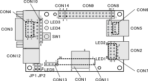
第5章 Interface Specifications5.1.1. Armadillo-420 Interface Layout表5.1 Armadillo-420 Interfaces | Part Number | Interface | Shape | Notes |
|---|
| CON1 | microSD slot | Hinge type | | | CON2 | LAN Interface | RJ-45 | | | CON3 | Serial interface | D-Sub 9 pin (male) | | | CON4 | Serial interface | 10 pin (2.54mm pitch) | Signal lines shared with CON3 | | CON5 | USB interface | Type-A 2 port stack | | | CON6 | USB interface | 4 pin (2mm pitch) | Signal lines shared with lower port of CON5 | | CON7 | LAN Interface | 10 pin (2.54mm pitch) | Some signal lines shared with CON2 | | CON8 | Ext. reset terminal | 2 pin (2.54mm pitch) | | | CON9 | Expansion Interface 1 | 28 pin (2.54mm pitch) | | | CON10 | i.MX257 JTAG interface | 8 pin (2.54mm pitch) | | | CON12 | Power in connector | DC jack | | | CON13 | Power in connector | 4 pin (2.54 mm pitch) | | | CON14 | Expansion Interface 2 | 4 pin (2.54 mm pitch) | | | LED1 | Link LED (green) | Surface mounted LCD | Shown on upper part of CON2 | | LED2 | Activity LED (yellow) | Surface mounted LCD | Shown on upper part of CON2 | | LED3 | User LED (red) | φ3mm LED | | | LED4 | User LED (green) | φ3mm LED | | | LED5 | User LED (yellow) | Surface mounted LCD | | | SW1 | User switch | Tact Switch h=17mm | | | JP1 | Boot mode jumper | 2 pin (2.54mm pitch) | | | JP2 | User jumper | 2 pin (2.54mm pitch) | |
5.1.2. Armadillo-440 Interface Layout表5.2 Armadillo-440 Interfaces | Part Number | Interface | Shape | Notes |
|---|
| CON1 | microSD slot | Hinge type | | | CON2 | LAN Interface | RJ-45 | | | CON3 | Serial interface | D-Sub 9 pin (male) | | | CON4 | Serial interface | 10 pin (2.54mm pitch) | Signal lines shared with CON3 | | CON5 | USB interface | Type-A 2 port stack | | | CON6 | USB interface | 4 pin (2mm pitch) | Signal lines shared with lower port of CON5 | | CON7 | LAN Interface | 10 pin (2.54mm pitch) | Some signal lines shared with CON2 | | CON8 | Ext. reset terminal | 2 pin (2.54mm pitch) | | | CON9 | Expansion Interface 1 | 28 pin (2.54mm pitch) | | | CON10 | i.MX257 JTAG interface | 8 pin (2.54mm pitch) | | | CON11 | LCD Interface | 50 pin (0.5mm pitch) | | | CON12 | Power in connector | DC jack | | | CON13 | Power in connector | 4 pin (2.54 mm pitch) | | | CON14 | Expansion Interface 2 | 4 pin (2.54 mm pitch) | | | LED1 | Link LED (green) | Surface mounted LCD | Shown on upper part of CON2 | | LED2 | Activity LED (yellow) | Surface mounted LCD | Shown on upper part of CON2 | | LED3 | User LED (red) | φ3mm LED | | | LED4 | User LED (green) | φ3mm LED | | | LED5 | User LED (yellow) | Surface mounted LCD | | | SW1 | User switch | Tact Switch h=17mm | | | JP1 | Boot mode jumper | 2 pin (2.54mm pitch) | | | JP2 | User jumper | 2 pin (2.54mm pitch) | |
5.2. Electrical SpecificationsThe electrical specifications of the input/output interfaces are shown in 表5.4「Input/Output Interface Electrical Specifications」. With the Software Pad Control (SW_PAD_CTL) and Drive Voltage Select Group Control (SW_PAD_CTL_GRP_DVS) registers in i.MX257 it is possible to alter the output current (Std, High, Max), slew rate (Slow, Fast), and pull-up/pull-down. 表5.3 Input/Output Interface Rated Absolute Maximum | Symbol | Parameter | Min | Max | Units |
|---|
| VImax | Input voltage range | –0.5 | OVDD+0.3 | V |
表5.4 Input/Output Interface Electrical Specifications | Symbol | Parameter | Min | Max | Units | Conditions |
|---|
| VIH | CMOS High-Level Input Voltage | 0.7 x OVDD | OVDD | V | OVDD = +3.3V | | VIL | CMOS Low-Level Input Voltage | -0.3 | 0.3 x OVDD | V | OVDD = +3.3V | | VOH | CMOS High-Level Output Voltage | OVDD-0.15 | | V | IOH = -1mA | | 0.8 x OVDD | | V | IOH = Specified Drive | | VOL | CMOS Low-Level Output Voltage | | 0.15 | V | IOL = 1mA | | | 0.2 x OVDD | V | IOL = Specified Drive | | IOH_S | High-Level Output Current, Slow Slew Rate | -2.0 | | mA | VOH = 0.8 x OVDD, Std Drive | | -4.0 | | mA | VOH = 0.8 x OVDD, High Drive | | -8.0 | | mA | VOH = 0.8 x OVDD, Max Drive | | IOH_F | High-Level Output Current, Fast Slew Rate | -4.0 | | mA | VOH = 0.8 x OVDD, Std Drive | | -6.0 | | mA | VOH = 0.8 x OVDD, High Drive | | -8.0 | | mA | VOH = 0.8 x OVDD, Max Drive | | IOL_S | Low-Level Output Current, Slow Slew Rate | 2.0 | | mA | VOL = 0.2 x OVDD, Std Drive | | 4.0 | | mA | VOL = 0.2 x OVDD, High Drive | | 8.0 | | mA | VOL = 0.2 x OVDD, Max Drive | | IOL_F | Low-Level Output Current, Fast Slew Rate | 4.0 | | mA | VOH = 0.2 x OVDD, Std Drive | | 6.0 | | mA | VOH = 0.2 x OVDD, High Drive | | 8.0 | | mA | VOH = 0.2 x OVDD, Max Drive | | IIN | Input Current (no PU/PD[]) | | 0.1 | μA | VI = 0 | | | 0.06 | μA | VI = OVDD = +3.3V | | Input Current (22kΩPU) | 117 | 184 | μA | VI = 0 | | 0.0001 | 0.0001 | μA | VI = OVDD = +3.3V | | Input Current (47kΩPU) | 54 | 88 | μA | VI = 0 | | 0.0001 | 0.0001 | μA | VI = OVDD = +3.3V | | Input Current (100kΩPU) | 25 | 42 | μA | VI = 0 | | 0.0001 | 0.0001 | μA | VI = OVDD = +3.3V | | Input Current (100kΩPD) | 0.0001 | 0.0001 | μA | VI = 0 | | 25 | 42 | μA | VI = OVDD = +3.3V | | ICC | High-impedance Supply Current | | 1.2 | μA | VI = 0 | | | 1.2 | μA | VI = OVDD = +3.3V |
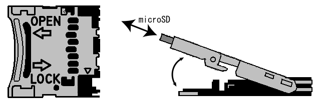
CON1 is a microSD/microMMC slot connected to a SD/MMC controller (SDHC1) in i.MX257. microSD card power supply can be controlled[] with the NFRE_B (GPIO3_27) pin on i.MX257. 表5.5 CON1 Signals | Pin Number | Signal Name | I/O | Function |
|---|
| 1 | SD1_DAT2 | In/Out | Data bus (bit 2), connected to SD1_DATA2 pin on i.MX257 | | 2 | SD1_DAT3 | In/Out | Data bus (bit 3), connected to SD1_DATA3 pin on i.MX257 | | 3 | SD1_CMD | In/Out | Command / Response, connected to SD1_CMD pin on i.MX257 | | 4 | VDD | Power | Power (+3.3V_CPU)[] | | 5 | SD1_CLK | Out | Clock, connected to SD1_CLK pin on i.MX257 | | 6 | VSS | Power | Power (GND) | | 7 | SD1_DAT0 | In/Out | Data bus (bit 0), connected to SD1_DATA0 pin on i.MX257 | | 8 | SD1_DAT1 | In/Out | Data bus (bit 1), connected to SD1_DATA1 pin on i.MX257 | | 9 | SD1_CD* | In | Card detect (low: card inserted, high: card ejected) connected to NFRB (GPIO3_31) pin on i.MX257 |
CON1 is a hinge type connector. The cover on the connector must be opened in order to insert and remove the card. When opening, the cover should first be unlocked by sliding the upper part of the connector horizontally in the directory shown by the OPEN arrow. ![[警告]](images/warning.png) | |
|---|
CON1 is not hot-pluggable. Be sure to turn off the power supply before inserting or removing a microSD card. |
| |
|---|
Please ensure to leave the cover on CON1 in a locked state, regardless of whether a microSD card is inserted or not. If the cover is left unlocked when a microSD is not inserted, the internal contact of the connector may come into contact with the cover and cause the board to reset. |
![[ティップ]](images/tip.png) | |
|---|
Information on tested microSD / microMMC cards is available on the Armadillo Developers Site and is updated regularly. |
5.4. CON2, CON7 (LAN Interface)CON2 and CON7 are a 10BASE-T/100BASE-TX LAN interface which can be used with Category 5 or above Ethernet cables. The interface includes AUTO-MDIX functionality allowing it to automatically detect straight or cross cable connections and swap the send and receive terminals accordingly. 表5.6 CON2 Signals | Pin Number | Signal Name | I/O | Function |
|---|
| 1 | TX+ | Out | Differential twisted pair transmit (+), signal line shared with CON7 (pin 1) | | 2 | TX- | Out | Differential twisted pair transmit (-), signal line shared with CON7 (pin 4) | | 3 | RX+ | In | Differential twisted pair receive (+), signal line shared with CON7 (pin 3) | | 4 | - | - | 75Ω terminal after connection with CON2 (pin 5), signal line shared with CON7 (pin 5) | | 5 | - | - | 75Ω terminal after connection with CON2 (pin 4), signal line shared with CON7 (pin 5) | | 6 | RX- | In | Differential twisted pair receive (-), signal line shared with CON7 (pin 6) | | 7 | - | - | 75Ω terminal after connection with CON2 (pin 8), signal line shared with CON7 (pin 7) | | 8 | - | - | 75Ω terminal after connection with CON2 (pin 7), signal line shared with CON7 (pin 7) |
表5.7 CON7 Signals | Pin Number | Signal Name | I/O | Function |
|---|
| 1 | TX+ | Out | Differential twisted pair transmit (+), signal line shared with CON2 (pin 1) | | 2 | ACTIVITY_LED | Out | Activity indicator (low: data transmit/receive, high: no data) | | 3 | RX+ | In | Differential twisted pair receive (+), signal line shared with CON2 (pin 3) | | 4 | TX- | Out | Differential twisted pair transmit (-), signal shared with CON2 (pin 2) | | 5 | - | - | 75Ω terminal, signal line shared with CON2 (pins 4, 5) | | 6 | RX- | In | Differential twisted pair receive (-), signal line shared with CON2 (pin 6) | | 7 | - | - | 75Ω terminal, signal line shared with CON2 (pins 7, 8) | | 8 | LINK_LED | - | Link indicator (low: link established, high: no link) | | 9 | +3.3V_CPU | Power | Power (+3.3V_CPU)[] | | 10 | GND | Power | Power (GND) |
| |
|---|
As CON2 and CON7 share the same signal lines they cannot both be used at the same time. Please be sure to use only one of the connectors. |
5.5. CON3, CON4 (Serial Interface)CON3 and CON4 are an asynchronous serial interface connected to a UART controller in the i.MX257. Although CON3 and CON4 have differing connector types and pin layouts, they share the same serial signal lines. Signal input/output levels: RS232C levels Max data rate: 230.4kbps Flow control: CTS, RTS, DTR, DSR, DCD, RI Controller: i.MX257 internal UART controller (UART2) CON3 connector type: D-Sub 9 pin CON4 connector type: 10 pin (2x5, 2.54mm pitch)
It is possible to shut down the RS232C level conversion IC connected to CON3 and CON4 by controlling[] the BOOT_MODE1 (GPIO4_31) pin on the i.MX257. 表5.8 CON3 Signals | Pin Number | Signal Name | I/O | Function |
|---|
| 1 | DCD2 | In | Carrier Detect, connected to the UART1_RTS pin on i.MX257, signal line shared with CON4 (pin 1) | | 2 | RXD2 | In | Receive Data, connected to the UART2_RXD pin on i.MX257, signal line shared with CON4 (pin 3) | | 3 | TXD2 | Out | Transmit Data, connected to UART2_TXD pin on i.MX257, signal line shared with CON4 (pin 5) | | 4 | DTR2 | Out | Data Terminal Ready, connected to UART1_RXD on i.MX257, signal line shared with CON4 (pin 7) | | 5 | GND | Power | Power (GND) | | 6 | DSR2 | In | Data Set Ready, connected to UART1_TXD pin on i.MX257, signal line shared with CON4 (pin 2) | | 7 | RTS2 | Out | Request To Send, connected to UART2_CTS pin on i.MX257, signal line shared with CON4 (pin 4) | | 8 | CTS2 | In | Clear To Send, connected to UART2_RTS pin on i.MX257, signal line shared with CON4 (pin 6) | | 9 | RI2 | In | Ring Indicator, connected to UART1_CTS pin on i.MX257, signal line shared with CON4 (pin 8) |
表5.9 CON4 Signals | Pin Number | Signal Name | I/O | Function |
|---|
| 1 | DCD2 | In | Carrier Detect, connected to the UART1_RTS pin on i.MX257, signal line shared with CON3 (pin 1) | | 2 | DSR2 | In | Data Set Ready, connected to UART1_TXD pin on i.MX257, signal line shared with CON3 (pin 6) | | 3 | RXD2 | In | Receive Data, connected to the UART2_RXD pin on i.MX257, signal line shared with CON3 (pin 2) | | 4 | RTS2 | Out | Request To Send, connected to UART2_CTS pin on i.MX257, signal line shared with CON3 (pin 7) | | 5 | TXD2 | Out | Transmit Data, connected to UART2_TXD pin on i.MX257, signal line shared with CON3 (pin 3) | | 6 | CTS2 | In | Clear To Send, connected to UART2_RTS pin on i.MX257, signal line shared with CON3 (pin 8) | | 7 | DTR2 | Out | Data Terminal Ready, connected to UART1_RXD on i.MX257, signal line shared with CON3 (pin 4) | | 8 | RI2 | In | Ring Indicator, connected to UART1_CTS pin on i.MX257, signal line shared with CON3 (pin 9) | | 9 | GND | Power | Power (GND) | | 10 | +3.3V_CPU | Power | Power (+3.3V_CPU)[] |
| |
|---|
As CON3 and CON4 share the same signal lines they cannot both be used at the same time. Please be sure to use only one of the connectors. |
5.6. CON5, CON6 (USB Interface)CON5 is a USB interface connected to a USB controller in the i.MX257. Although the lower port of CON5 and CON6 have differing connector types and pin layouts, they share the same USB signal lines. It is possible to select between the power in (VIN) of CON12 (or CON13) and the +5V power generated by the power management IC (PMIC) as the source of power provided to USB devices from CON5 and CON6 by controlling[] the NFWE_B (GPIO3_26) pin on the i.MX257. When using a power input of less than 4.75V while connecting USB devices, please select the PMIC generated +5V power source. Please be aware that the total maximum current that can be supplied to the two USB channels is 300mA when using the PMIC generated +5V power source. [] CON5 Upper Port: Data transmission modes: USB 2.0 Full Speed (12Mbps), Low Speed (1.5Mbps) Controller: i.MX257 internal USB controller (HOST) PHY: i.MX257 internal USB PHY (USBPHY2)
CON5 Lower Port, CON6: Data transmission modes:USB 2.0 High Speed (480Mbps), Full Speed (12Mbps), Low Speed (1.5Mbps) Controller: i.MX257 internal USB controller (OTG) PHY: i.MX257 internal USB PHY (USBPHY1)
表5.10 CON5 Signals | Pin Number | Signal Name | I/O | Function |
|---|
| 1 | +5V_USB | Power | Selection between USB power and power in VIN (when above 4.75V) providing for a max 500mA supply | | 2 | USB1- | In/Out | USB1 minus side signal, i.MX257 USBPHY1_DM pin connection, signal line shared with CON6 (pin 2) | | 3 | USB1+ | In/Out | USB1 plus side signal, i.MX257 USBPHY1_DP pin connection, signal line shared with CON6 (pin 3) | | 4 | GND | Power | Power (GND) | | 5 | +5V_USB | Power | Selection between USB power and power in VIN (when above 4.75V) providing for a max 500mA supply | | 6 | USB2- | In/Out | USB2 minus side signal, i.MX257 USBPHY2_DM pin connection | | 7 | USB2+ | In/Out | USB2 plus side connection, i.MX257 USBPHY2_DP pin connection | | 8 | GND | Power | Power (GND) |
表5.11 CON6 Signals | Pin Number | Signal Name | I/O | Function |
|---|
| 1 | +5V_USB | Power | Selection between USB power and power in VIN (when above 4.75V) providing for a max 500mA supply | | 2 | USB1- | In/Out | USB1 minus side signal, i.MX257 USBPHY1_DM pin connection, signal line shared with CON5 (pin 2) | | 3 | USB1+ | In/Out | USB1 plus side signal, i.MX257 USBPHY1_DP pin connection, signal line shared with CON5 (pin 3) | | 4 | GND | Power | Power (GND) |
| |
|---|
As the lower port on CON5 and CON6 share the same signal lines they cannot both be used at the same time. Please be sure to use only one of the connectors. |
| |
|---|
Information on tested USB devices is available on the Armadillo Developers Site and is updated regularly. |
5.7. CON8 (External Reset Terminal)CON8 is an external reset terminal. CON8 (pin 1) is connected to the reset IC incorporated on the board, and while this signal is low the board will be placed in a reset state. 表5.12 CON8 Signals | Pin Number | Signal Name | I/O | Function |
|---|
| 1 | EXT_RESET* | In | External Reset (low[]: reset state, high[]: no reset) | | 2 | GND | Power | Power (GND) |
5.8. CON9 (Expansion Interface 1)CON9 is an expansion input/output interface. The line signals of the internal controllers in the i.MX257 can be used by configuring the i.MX257 multiplex function. For the initial state of each signal pin, please refer to 付録B Initial Configuration State of Expansion Interfaces. 表5.13 CON9 Signals | Pin Number | Signal Name | I/O | Function |
|---|
| 1 | EXT_IO0 | In/Out | Expansion I/O 0, connected to VSTBY_REQ pin on i.MX257 | | 2 | EXT_IO1 | In/Out | Expansion I/O 1, connected to RTCK pin on i.MX257 | | 3 | EXT_IO2 | In/Out | Expansion I/O 2, connected to CSPI1_MOSI pin on i.MX257 | | 4 | EXT_IO3 | In/Out | Expansion I/O 3, connected to CSI_D2 pin on i.MX257 | | 5 | EXT_IO4 | In/Out | Expansion I/O 4, connected to CSPI1_MISO pin on i.MX257 | | 6 | EXT_IO5 | In/Out | Expansion I/O 5, connected to CSI_D3 pin on i.MX257 | | 7 | +3.3V_IO | Power | Power (+3.3V_IO) | | 8 | +3.3V_IO | Power | Power (+3.3V_IO) | | 9 | GND | Power | Power (GND) | | 10 | GND | Power | Power (GND) | | 11 | EXT_IO6 | In/Out | Expansion I/O 6, connected to CSPI1_SS1 pin on i.MX257 | | 12 | EXT_IO7 | In/Out | Expansion I/O 7, connected to CSI_D4 pin on i.MX257 | | 13 | EXT_IO8 | In/Out | Expansion I/O 8, connected to CSPI1_SCLK pin on i.MX257 | | 14 | EXT_IO9 | In/Out | Expansion I/O 9, connected to CSI_D5 pin on i.MX257 | | 15 | EXT_IO10 | In/Out | Expansion I/O 10, connected to CSI_D8 pin on i.MX257 | | 16 | EXT_IO11 | In/Out | Expansion I/O 11, connected to CSI_D6 pin on i.MX257 | | 17 | EXT_IO12 | In/Out | Expansion I/O 12, connected to CSI_D9 pin on i.MX257 | | 18 | EXT_IO13 | In/Out | Expansion I/O 13, connected to CSI_D7 pin on i.MX257 | | 19 | GND | Power | Power (GND) | | 20 | +3.3V_IO | Power | Power (+3.3V_IO) | | 21 | EXT_IO14 | In/Out | Expansion I/O 14, connected to CSI_MCLK pin on i.MX257 | | 22 | EXT_IO15 | In/Out | Expansion I/O 15, connected to CSI_VSYNC pin on i.MX257 | | 23 | EXT_IO16 | In/Out | Expansion I/O 16, connected to CSI_HSYNC pin on i.MX257 | | 24 | EXT_IO17 | In/Out | Expansion I/O 17, connected to CSI_PIXCLK pin on i.MX257 | | 25 | EXT_IO18 | In/Out | Expansion I/O 18, connected to CSPI1_SS0 pin on i.MX257 | | 26 | EXT_IO19 | In/Out | Expansion I/O 19, connected to CSPI1_RDY pin on i.MX257 | | 27 | EXT_IO20 | In/Out | Expansion I/O 20, connected to CLKO pin on i.MX257 | | 28 | EXT_IO21 | In/Out | Expansion I/O 21, connected to EXT_ARMCLK pin on i.MX257 |
表5.14 CON9 Signal Multiplex | Pin Number | Signal Name | Multiplex Modes[] |
|---|
| ALT0 | ALT1 | ALT2 | ALT5 | ALT7 |
|---|
| 1 | EXT_IO0 | | | | GPIO3_17 | | | 2 | EXT_IO1 | | 1-WIRE | | GPIO3_14 | | | 3 | EXT_IO2 | CSPI1_MOSI | | UART3_RXD | GPIO1_14 | | | 4 | EXT_IO3 | CSI_D2 | UART5_RXD | SD2_DAT4 | GPIO1_27 | CSPI3_MOSI | | 5 | EXT_IO4 | CSPI1_MISO | | UART3_TXD | GPIO1_15 | | | 6 | EXT_IO5 | CSI_D3 | UART5_TXD | SD2_DAT5 | GPIO1_28 | CSPI3_MISO | | 7 | +3.3V_IO | | | | | | | 8 | +3.3V_IO | | | | | | | 9 | GND | | | | | | | 10 | GND | | | | | | | 11 | EXT_IO6 | CSPI1_SS1 | | UART3_RTS | GPIO1_17 | | | 12 | EXT_IO7 | CSI_D4 | UART5_RTS | SD2_DAT6 | GPIO1_29 | CSPI3_SCLK | | 13 | EXT_IO8 | CSPI1_SCLK | | UART3_CTS | GPIO1_18 | | | 14 | EXT_IO9 | CSI_D5 | UART5_CTS | SD2_DAT7 | GPIO1_30 | CSPI3_RDY | | 15 | EXT_IO10 | CSI_D8 | | AUD6_RXC | GPIO1_7 | CSPI3_SS2 | | 16 | EXT_IO11 | CSI_D6 | | SD2_CMD | GPIO1_31 | CSPI3_SS0 | | 17 | EXT_IO12 | CSI_D9 | | AUD6_RXFS | GPIO4_21 | CSPI3_SS3 | | 18 | EXT_IO13 | CSI_D7 | | SD2_CLK | GPIO1_6 | CSPI3_SS1 | | 19 | GND | | | | | | | 20 | +3.3V_IO | | | | | | | 21 | EXT_IO14 | CSI_MCLK | AUD6_TXD | SD2_DAT0 | GPIO1_8 | | | 22 | EXT_IO15 | CSI_VSYNC | AUD6_RXD | SD2_DAT1 | GPIO1_9 | | | 23 | EXT_IO16 | CSI_HSYNC | AUD6_TXC | SD2_DAT2 | GPIO1_10 | | | 24 | EXT_IO17 | CSI_PIXCLK | AUD6_TXFS | SD2_DAT3 | GPIO1_11 | | | 25 | EXT_IO18 | CSPI1_SS0 | | PWMO2 | GPIO1_16 | | | 26 | EXT_IO19 | CSPI1_RDY | | | GPIO2_22 | | | 27 | EXT_IO20 | CLKO | | | GPIO2_21 | | | 28 | EXT_IO21 | | | | GPIO3_15 | |
5.9. CON10 (i.MX257 JTAG Interface)CON10 is an interface for connecting JTAG debuggers. It is connected to the JTAG Controller in the i.MX257. It is possible to convert this interface to the standard ARM 20 pin layout with the JTAG Conversion Cable (OP-JC8P25-00) option. For details, please see 付録A JTAG Conversion Cable (OP-JC8P25-00). 表5.15 CON10 Signals | Pin Number | Signal Name | I/O | Function |
|---|
| 1 | +3.3V_CPU | Power | Power (+3.3V_CPU)[] | | 2 | JTAG_TRST* | In | Test Reset, connected to TRSTB pin on i.MX257 | | 3 | JTAG_TDI | In | Test Data In, connected to TDI pin on i.MX257 | | 4 | JTAG_TMS | In | Test Mode Select, connected to TMS pin on i.MX257 | | 5 | JTAG_TCK | In | Test Clock, connected to TCK pin on i.MX257 | | 6 | JTAG_TDO | Out | Test Data Out, connected to TDO pin on i.MX257 | | 7 | CPU_RESET* | In | i.MX257 reset[], connected to RESET_B pin on i.MX257 | | 8 | GND | Power | Power (GND) |
5.10. CON11 (LCD Interface)CON11 is a LCD interface which connects to LCD modules with digital RGB inputs. It has connections to a number of functions in the i.MX257, including the LCD controller and touch screen controller. For the initial state of each signal pin, please refer to 付録B Initial Configuration State of Expansion Interfaces. Max resolution: 800x600 (18bit) Supported touch screens: 4-Wire Resistive Connector Type: 50 pin FFC connector (0.5mm pitch)
表5.16 CON11 Signals | Pin Number | Signal Name | I/O | Function |
|---|
| 1 | VIN | Power | Power (CON12 or CON13 power in) | | 2 | VIN | Power | Power (CON12 or CON13 power in) | | 3 | VIN | Power | Power (CON12 or CON13 power in) | | 4 | +3.3V_IO | Power | Power (+3.3V_IO) | | 5 | +3.3V_IO | Power | Power (+3.3V_IO) | | 6 | GND | Power | Power (GND) | | 7 | GND | Power | Power (GND) | | 8 | LCD_LSCLK | Out | Connected to LSCLK pin on i.MX257 | | 9 | LCD_HSYN | Out | Connected to HSYNC pin on i.MX257 | | 10 | LCD_VSYN | Out | Connected to VSYNC pin on i.MX257 | | 11 | LCD_OE_ACD | Out | Connected to OE_ACD pin on i.MX257 | | 12 | PWMO1 | Out | Connected to PWM pin on i.MX257 | | 13 | LCD_LD0 | Out | Connected to LD0 pin on i.MX257 | | 14 | LCD_LD1 | Out | Connected to LD1 pin on i.MX257 | | 15 | LCD_LD2 | Out | Connected to LD2 pin on i.MX257 | | 16 | LCD_LD3 | Out | Connected to LD3 pin on i.MX257 | | 17 | LCD_LD4 | Out | Connected to LD4 pin on i.MX257 | | 18 | LCD_LD5 | Out | Connected to LD5 pin on i.MX257 | | 19 | GND | Power | Power (GND) | | 20 | LCD_LD6 | Out | Connected to LD6 pin on i.MX257 | | 21 | LCD_LD7 | Out | Connected to LD7 pin on i.MX257 | | 22 | LCD_LD8 | Out | Connected to LD8 pin on i.MX257 | | 23 | LCD_LD9 | Out | Connected to LD9 pin on i.MX257 | | 24 | LCD_LD10 | Out | Connected to LD10 pin on i.MX257 | | 25 | LCD_LD11 | Out | Connected to LD11 pin on i.MX257 | | 26 | GND | Power | Power (GND) | | 27 | LCD_LD12 | Out | Connected to LD12 pin on i.MX257 | | 28 | LCD_LD13 | Out | Connected to LD13 pin on i.MX257 | | 29 | LCD_LD14 | Out | Connected to LD14 pin on i.MX257 | | 30 | LCD_LD15 | Out | Connected to LD15 pin on i.MX257 | | 31 | LCD_LD16 | Out | Connected to GPIO_E pin on i.MX257 | | 32 | LCD_LD17 | Out | Connected to GPIO_F pin on i.MX257 | | 33 | GND | Power | Power (GND) | | 34 | TOUCH_XP | In/Out | Connected to XP pin on i.MX257 | | 35 | TOUCH_XN | In/Out | Connected to XN pin on i.MX257 | | 36 | TOUCH_YP | In/Out | Connected to YP pin on i.MX257 | | 37 | TOUCH_YN | In/Out | Connected to YN pin on i.MX257 | | 38 | GND | Power | Power (GND) | | 39 | EXT_IO24 | In/Out | Expansion I/O 24, connected to DE_B pin on i.MX257 | | 40 | EXT_IO25 | In/Out | Expansion I/O 25, connected to KPP_ROW0 pin on i.MX257 | | 41 | EXT_IO26 | In/Out | Expansion I/O 26, connected to KPP_ROW1 pin on i.MX257 | | 42 | EXT_IO27 | In/Out | Expansion I/O 27, connected to KPP_ROW2 pin on i.MX257 | | 43 | EXT_IO28 | In/Out | Expansion I/O 28, connected to KPP_ROW3 pin on i.MX257 | | 44 | EXT_IO29 | In/Out | Expansion I/O 29, connected to KPP_COL0 pin on i.MX257 | | 45 | EXT_IO30 | In/Out | Expansion I/O 30, connected to KPP_COL1 pin on i.MX257 | | 46 | EXT_IO31 | In/Out | Expansion I/O 31, connected to KPP_COL2 pin on i.MX257 | | 47 | EXT_IO32 | In/Out | Expansion I/O 32, connected to KPP_COL3 pin on i.MX257 | | 48 | EXT_IO33 | In/Out | Expansion I/O 33, connected to GPIO_A pin on i.MX257 | | 49 | EXT_IO34 | In/Out | Expansion I/O 34, connected to GPIO_B pin on i.MX257 | | 50 | GND | Power | Power (GND) |
表5.17 CON11 Signal Multiplex | Pin Number | Signal Name | Multiplex Modes[] |
|---|
| ALT0 | ALT1 | ALT2 | ALT3 | ALT4 | ALT5 |
|---|
| 1 | VIN | | | | | | | | 2 | VIN | | | | | | | | 3 | VIN | | | | | | | | 4 | +3.3V_IO | | | | | | | | 5 | +3.3V_IO | | | | | | | | 6 | GND | | | | | | | | 7 | GND | | | | | | | | 8 | LCD_LSCLK | LSCLK | SLCDC_CS | | | | | | 9 | LCD_HSYN | HSYN | | | | | | | 10 | LCD_VSYN | VSYN | | | | | | | 11 | LCD_OE_ACD | OE_ACD | SLCDC_RS | | | | | | 12 | PWMO1 | | | | | | | | 13 | LCD_LD0 | LD0 | SLCDC_D0 | | | | | | 14 | LCD_LD1 | LD1 | SLCDC_D1 | | | | | | 15 | LCD_LD2 | LD2 | SLCDC_D2 | | | | | | 16 | LCD_LD3 | LD3 | SLCDC_D3 | | | | | | 17 | LCD_LD4 | LD4 | SLCDC_D4 | | | | | | 18 | LCD_LD5 | LD5 | SLCDC_D5 | | | | | | 19 | GND | | | | | | | | 20 | LCD_LD6 | LD6 | SLCDC_D6 | | | | | | 21 | LCD_LD7 | LD7 | c | | | | | | 22 | LCD_LD8 | LD8 | SLCDC_D8 | | | | | | 23 | LCD_LD9 | LD9 | SLCDC_D9 | | | | | | 24 | LCD_LD10 | LD10 | SLCDC_D10 | | | | | | 25 | LCD_LD11 | LD11 | SLCDC_D11 | | | | | | 26 | GND | | | | | | | | 27 | LCD_LD12 | LD12 | SLCDC_D12 | | | | | | 28 | LCD_LD13 | LD13 | SLCDC_D13 | | | | | | 29 | LCD_LD14 | LD14 | SLCDC_D14 | | | | | | 30 | LCD_LD15 | LD15 | SLCDC_D15 | | | | | | 31 | LCD_LD16 | | | LD16 | | | | | 32 | LCD_LD17 | | | LD17 | | | | | 33 | GND | | | | | | | | 34 | TOUCH_XP | XP | | | | | | | 35 | TOUCH_XN | XN | | | | | | | 36 | TOUCH_YP | YP | | | | | | | 37 | TOUCH_YN | XN | | | | | | | 38 | GND | | | | | | | | 39 | EXT_IO24 | | | | | | GPIO2_20 | | 40 | EXT_IO25 | ROW0 | UART3_RXD | | | | GPIO2_29 | | 41 | EXT_IO26 | ROW1 | UART3_TXD | | | | GPIO2_30 | | 42 | EXT_IO27 | ROW2 | UART3_RTS | AUD5_RXC | | | GPIO2_31 | | 43 | EXT_IO28 | ROW3 | UART3_CTS | AUD5_RXFS | | | GPIO3_0 | | 44 | EXT_IO29 | COL0 | UART4_RXD | AUD5_TXD | | | GPIO3_1 | | 45 | EXT_IO30 | COL1 | UART4_TXD | AUD5_RXD | | | GPIO3_2 | | 46 | EXT_IO31 | COL2 | UART4_RTS | AUD5_TXC | | | GPIO3_3 | | 47 | EXT_IO32 | COL3 | UART4_CTS | AUD5_TXFS | | | GPIO3_4 | | 48 | EXT_IO33 | GPIO1_0 | PWMO2 | | ROW4 | I2C3_SCL | | | 49 | EXT_IO34 | GPIO1_1 | PWMO3 | | ROW5 | I2C3_SDA | | | 50 | GND | | | | | | |
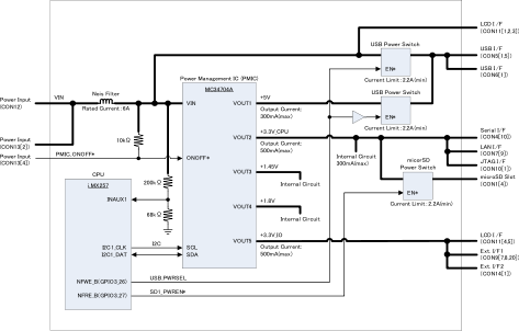
5.11. CON12, CON13 (Power In Connector)CON12 is a DC jack which supplies power to the board. The AC adapter jack type is EIAJ RC-5320A compliant (voltage classification 2). Jacks with the same polarity mark as 図5.6「AC Adapter Polarity Mark」 can be used. CON13 is a connector which supplies power to the board. Signal lines to control the power management IC (PMIC) on/off are included in this connector. 表5.18 CON13 Signals | Pin Number | Signal Name | I/O | Function |
|---|
| 1 | GND | Power | Power (GND) | | 2 | VIN | Power | Power in terminal, line shared with center pin of CON12 | | 3 | GND | Power | Power (GND) | | 4 | PMIC_ONOFF* | In | PMIC ON/OFF control (2sec or longer GND short to power off, GND short again to power back on)[] |
| |
|---|
CON12 and CON13 accept a power in voltage range of DC3.1V to 5.25V. Do not apply a voltage higher than 5.25V as this may damage the internal devices. |
| |
|---|
As the power lines of CON12 and CON13 are connected they cannot both be used at the same time. Please be sure to only supply power with one of the connectors. |
5.12. CON14 (Expansion Interface 2)CON14 is an expansion input/output interface. The line signals of the internal controllers in the i.MX257 can be used by configuring the i.MX257 multiplex function. For the initial state of each signal pin, please refer to 付録B Initial Configuration State of Expansion Interfaces. 表5.19 CON14 Signals | Pin Number | Signal Name | I/O | Function |
|---|
| 1 | +3.3V_IO | Power | Power (+3.3V_IO) | | 2 | GND | Power | Power (GND) | | 3 | EXT_IO22 | In/Out | Expansion I/O 22, connected to GPIO_C pin on i.MX257 | | 4 | EXT_IO23 | In/Out | Expansion I/O 23, connected to GPIO_D pin on i.MX257 |
表5.20 CON14 Signal Multiplex | Pin Number | Signal Name | Multiplex Modes[] |
|---|
| ALT0 | ALT1 | ALT2 | ALT5 | ALT6 |
|---|
| 1 | +3.3V_IO | | | | | | | 2 | GND | | | | | | | 3 | EXT_IO22 | GPIO1_2 | PWMO4 | I2C2_SCL | CSPI1_SS2 | CAN2_TX | | 4 | EXT_IO23 | GPIO1_3 | | I2C2_SDA | | CAN2_RX |
5.13. LED1, LED2 (LAN LEDs)LED1 and LED2 are the LAN interface status LEDs. They are shown on the upper part of CON2. 表5.21 LAN LED Meanings | LED | Name (color) | On | Off |
|---|
| LED1 | Link LED (green) | A LAN cable is connected and a 10BASE-T or 100BASE-TX link has been established. | A LAN cable is not connected or the LAN status of the connected device is not active. | | LED2 | Activity LED (yellow) | Data transmit/receive | No data |
5.14. LED3, LED4, LED5 (User LEDs)LED3, LED4 and LED5 are LEDs which can be used freely by the user. They can be controlled once the i.MX257 signals to which the LEDs are connected to are set to GPIO output mode. 表5.22 User LED Functions | LED | Name (color) | Function |
|---|
| LED3 | User LED (red) | Connected to NFALE (GPIO3_28) pin on i.MX257 (low: off, high: on) | | LED4 | User LED (green) | Connected to NFCLE (GPIO3_29) pin on i.MX257 (low: off, high: on) | | LED5 | User LED (yellow) | Connected to BOOT_MODE0 (GPIO4_30) pin on i.MX257 (low: off, high: on) |
| |
|---|
LED5 is connected to the same signal as JP1. LED5 cannot be controlled while JP1 is shorted. |
SW1 is a switch which can be freely used by the user. The switch status can be obtained once the i.MX257 signal it is connected to is set to GPIO input mode. 表5.23 User Switch Function | SW | Function |
|---|
| SW1 | Connected to NFWP_B (GPIO3_30) pin on i.MX257 (low: switch pressed, high: switch not pressed) |
5.16. JP1 (Boot Mode Configuration Jumper)The JP1 jumper is used to configure the board's boot mode. The boot mode is determined at power on time according to the jumper state. 表5.24 Boot Mode Configuration Jumper Behavior | JP1 | Behavior |
|---|
| Open | On-board flash memory boot | | Shorted | UART boot: UART2 (CON3 or CON4) |
| |
|---|
JP1 is connected to the same signal as LED5. Please do not use JP1 in a shorted state after booting to on-board flash memory. |
The JP2 jumper can be used freely by the user. The jumper status can be obtained once the i.MX257 signal it is connected to is set to GPIO input mode. 表5.25 User Jumper Function | JP | Function |
|---|
| JP2 | Connected to NF_CE0 (GPIO3_22) on i.MX257 (low: shorted, high: open) |
| |
|